Thursday 28 November 2013

Metal Oxide Varistor (MOV)

Was checking about transient suppressors, whether it be spikes or surges and one device that came to mind was TVS diode. The other alternatives are spark gaps and MOV. Before going other let us get clarified what basically a transient is. A transient is nothing but a high voltage compared to normal operating voltage of a circuit which can be termed spike or surge based on the time period it is present. Termed spike if it is for lesser time. A surge if it exists for a long duration.

When a transient hits a circuit, it may lead to catastrophic events like electronics component damage and in some cases burning. So, as a designer it is must to take care in design phase itself to include protection for transients. Protection can be done either by using MOV, spark gap or a TVS diode.

What is the basic difference between TVS diode, MOV and spark gap? 

TVS diode has low clamping voltages. So, it is suitable for a circuit and helps circuit not to get damaged by over voltages. MOV has higher clamping voltage and is able to carry more current than a TVS diode. We have discussed about spark gaps previously in the blog. Just reminding again, a spark gap has very high breakdown voltage compared to MOV and TVS diode.


What is MOV?

MOV, short form for Metal oxide varistor is a nonlinear, voltage dependent device. Varistor sounds like a variation of resistance but in reality it is non ohmic variable resistor which is different from potentiometer (ohmic variation). MOV acts as transient voltage suppressor and is connected in parallel in a circuit at the input. Under normal input voltage conditions, MOV does not conduct. When transient occurs and input voltage reaches above breakdown voltage of MOV, it clamps voltage to safe level and shunts down the current. The power dissipated as heat in the device. MOV provides high resistance at a low voltage and low resistance at high voltage.


Symbol of Varistor:


MOV view:


How to increase the power handling capability of MOV?

MOVs must be connected in parallel to increase the power handling capacity. To increase the voltage handling capability, MOV must be connected in series. 

What is the internal configuration of MOV?

The configuration is like metal oxides between electrodes. These metal oxides from a back-to-back diodes and internally there are number of back-to-back diodes in parallel. 

Ratings of MOV:
  • Energy measured in Joules
  • Breakdown/Clamping Voltage
  • Capacitance Response time

Disadvantages of MOV:
  • Cannot handle high energies like lightning
  • Too much energy burns MOVs
  • Too many spikes degrades the MOV operation
  • Cannot control over current condition in a circuit
  • Higher clamping voltage, so, because of this lower over voltage conditions cannot be protected. For this, separate protection mechanism must be used which proves costly

Selection of MOV:

Take the case of a power line operating at 230 V AC. In this case, if you want to use a MOV, the best value if to use MOV which has breakdown between 260-275 V. Keep in mind that a power lines sometimes can have spike in the range of kV.


Advantages of MOV:
  • Cheap solution for protection
  • Easy integration to circuit
  • Can conduct more current compared to TVS diodes
  • Higher clamping voltage
  • Response time is less compared to Spark Gap

Tuesday 26 November 2013

Validation devices - Smart Tweezer

It is common to use a tweezer in our applications. we generally use it as a assistant for soldering components. What if such a tweezer has LCR measurement option. In such a case,  it will be such a handy device to have. Basically, it also can identify the type of component. What if you have a soldered complex board and you are debugging one. Validating or debugging such a board becomes easy if you have smart tweezer kind of device.

Smart tweezers are basically hand-held, which help in measurement and identification of components. this helps to improve your debug time. Select a smart tweezer as per the precision required. But if you take a LCR meter separately, it will have more accuracy than smart tweezer. Keeping aside that disadvantage, if you are starting on a board debug, make sure you have a smart tweezer in hand.

Friday 22 November 2013

Insulated Gate Bipolar Transistor (IGBT) - Part 1

Everyone of us sometime or the other might have used a switching device in our application. Whether it be diode, power diode, bipolar transistor, mosfet, thyristor, when our application demanded ON/OFF condition we have used either of these devices. We tend to select either of them based on the application need. Application need meant current capability, switching frequency, reverse voltage rating, etc. But when and where to use what, is another point of discussion.

Among such devices, Insulated Gate Bipolar Transistor (IGBT) is one. IGBT is basically a power semiconductor device used in medium to high power applications. IGBT has 4 layers (P-N-P-N) which reminds of SCR configuration. The power .handling capability of IGBT can be increased by connecting several IGBTs in parallel. It is a minority carrier device which uses majority as well as minority carriers.

As discussed, IGBT is used as a switch in many applications. Switching operation meant device will be operating in saturation and cut-off state and not in linear region. IGBT switches at a faster rate and also has higher efficiency. We have to note that the switching frequency is always less than a power MOSFET.

IGBT combines the high input impedance characteristic of mosfet with current carrying capability of bipolar transistor. When we talk in terms of power handling capability, IGBT is preferred to Diode, BJT and FET and has less power handling capacity then thyristor.

How to allow reverse current in IGBT?

IGBT does not allow reverse conduction. In case, a reverse current is desired a freewheeling diode is used in parallel to IGBT.

What is the differentiating point in terms of forward drop when compared to Power FET?

As we all know, MOSFET behaves as a resistor. The voltage drop is proportional to current. Where as IGBT voltage drop behavior is on a logarithmic scale to current. So, while choosing either mosfet or IGBT, consideration must be given to current capability and blocking voltage specifications.

Operation of IGBT:

IGBT has 4 alternating layers.

Equivalent circuit of IGBT:


Structure of IGBT:

Advantages of IGBT:

  • High power dissipation
  • High reverse breakdown voltage
  • Simple gate drive
  • High current
  • Low saturation voltage
  • Combination of MOSFET and bipolar transistor in single device
  • Rugged and tolerant to heavy loads

Disadvantages of IGBT:

  • High voltage drop (but lower than mosfet)
  • Low operating frequency because of current tail
Applications of IGBT:
  • Switched mode power supply, UPS
  • Traction motor circuit (Trains)
  • induction heating
  • Solar inverters

Wednesday 6 November 2013

Using crystals in embedded applications - Part 2

In the previous section, we have seen how to select external capacitors of a crystal based on parasitic and load capacitance of crystal. The selection of these capacitors, determine the frequency of operation. In this section let us see what the individual parts of crystal section are going to contribute to oscillation.


  • Inverter inside the processor/micro controller acts as Class AB amplifier
  • Inverter provides 180 degrees phase-shift
  • For oscillation to be stable, the phase-shift must be 360 degrees 
  • Additional 180 degrees phase-shift is provided by C1, C2
  • As per oscillation theory, closed loop gain must be greater >= 1 for oscillation to be maintained
  • Loop gain gets reduced by ESR, shunt capacitance and load capacitance
  • Select a crystal with load capacitance <= 12pF
  • More the load capacitance of the crystal, more the power dissipated
  • If frequency of oscillation is higher than desired, increase load capacitance to reduce it to desired level
  • If frequency of oscillation is lower than the desired, reduce the load capacitance value to get desired frequency

Serial ATA (SATA) interface - Part 1

SATA short form for Serial Advanced attachment interface is a serial bus interface for interconnection of storage devices to processor. If you know desktop ingredients, you must be familiar with names like PATA, SCSI, SAS interfaces. PATA short form for Parallel advanced attachment interface has been used in personal computers for connecting hard disk drive to processor. PATA is a parallel interface with up to 40-60 wires (16-bit wide data interface). As we all know the disadvantage with parallel interface is mainly the length of transmission. even though we can achieve higher data rates with parallel interface, the main disadvantage is the length of transmission. with PATA we can achieve only 45-90 cm distance. Also, PATA can work only up to 133 MHz rate and uses +5V for signalling (TTL). The same PATA interface can be shared by many drives but due to bulkiness of connector, sharing not recommended. PATA is also knows as IDE or ATA. Hard disk drives available in the market are of sizes 2.5", 3.5" and 1.8". 3.5" drives are used in desktops and 2.5" drives in net book.

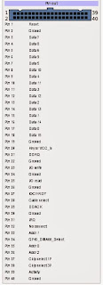
The below figures show PATA connectors, PATA HDD, PATA pin out.


Considering above points, a new interface came into existence which added serial features to SCSI (small computer system interface). It was called SAS short form for Serial attached SCSI. This basically can operate up to 1.5 GB/s and can have cables up to 8 meters long. this was used mainly for servers.

Now-a-days in desktops you don't see SCSI, PATA and SAS. A serial interface standard called SATA is seen. It differs from PATA in many ways and is not compatible in any ways. SATA is basically a serial interface standard which uses LVDS signalling for data transmission. There are various versions of SATA existing now like SATA 1.0, SATA 2.0, SATA 3.0 and SATA 4.0.

Electrical characteristics of SATA interface:
  • AC coupling capacitance of SATA is 12 pF
  • 100 ohm differential impedance
  • NRZ encoding
  • 8b/10b encoding
  • Transmit Rise/Fall time - 67-273 ps
  • 250mV differential LVDS signalling
Mechanical considerations of SATA interface:
  • SATA uses 7-pin data connector with appropriate grounding between differential lines
  • Uses 15-pin power connector, with staggered spin-up pin support
  • Uses +3.3V, +5V, +12V on the connector
  • Each pin in the connector carries 1.5 A current
  • Six standard ground pins on power connector
  • 1.27mm pitch connectors used
  • 1 meter length cable supported for SATA
The following figures show pin-outs for SATA power and Data connector


Some of the important points about SATA interface:
  • Capacitors on SATA line which are used for DC biasing are placed near to transmitter section
  • Hot plug supported in SATA interface
  • SATA supports data rates of 1.5 Gbps, 3 Gbps, 6 Gbps and 16 Gbps.
  • SATA uses I/O queuing protocol for efficient data transfer
  • In the evolution of any standard, to increase reuse of interface level hardware elated to ASIC, PHY, firmware same command will be used from previous versions of that standard. In SATA case also, command set from PATA has been retained.
  • If one wants to connect SATA device to a processor which doesn't have native SATA support, adapters are available. For example, if processor supports PATA, adapters can be used to connect SATA drive to processor
  • SATA Express is the latest standard of STA which supports up to 16 Gbps, this is done using native PCIe interface of the processor. A Mini PCIe support is enough on the board to connect a SATA express drive to board.
  • Observe the pins on SATA connector, you see them arranged in staggered manner. This helps to support hot plugging and improved mating
  • Wafer based connectors are used for SATA connectivity
  • A pin is reserved on power connector for SATA. This pin named as staggered spin up/activity is used to control drive spin on power up of unit. when staggered pin is pulled down by default, the drive spins as soon as the power is applied. This is little power consuming. Another case where staggered pin is pulled up. In this case, drive starts spinning, only when it is communicated to.
  • The mating count of these SATA connectors are restricted to less than 50.
  • SATA is half duplex interface
  • When SATA is not used, transmit pins float to the common mode voltage level

Monday 4 November 2013

Wireless charging - Part 1

Wireless charging is one of the recent innovations which involves charging without a direct connectivity. A charging mat or a sleeve kind of thing will be available which enables charging. The principle involves magnetic coupling between two coils. When a magnetic coil carrying current is placed near another magnetic coil, due to electro-magnetic induction, current will be induced in another coil. The current will be regulated to charge a battery using power management circuit. The following manufacturers produces chips for power management:

  • IDT
  • Texas Instruments
  • ON semiconductor
  • Freescale semiconductor
  • Qualcomm
  • NXP semiconductor
  • Panasonic


Several standards for wireless charging are in existence. the following are the list of these standards:
  • Qi
  • Power 2.0 by PMAT
  • A4WP
The main disadvantage of all these standards is the coupling factor. As the distance of the receiver gets separated more from transmitter, the coupling gets reduced and hence efficiency. This implies that distance from the coil should not exceed coil size. Another disadvantage is that receiver coil must be properly aligned with transmitter coil to get maximum transfer. A new standard by PMAT named Witricity enables the distance from coil exceeding more compared to coil size. This is like charging anywhere in the room.

Standards like A4WP are supported by companies like Intel which can be used in it's smartphone, laptops and net book. Considering the standard, Qi operates in the range 100-205 KHz and Power2.0 operates in the range 277-357 KHz.


Some of the existing products with wireless charging capability:
  • Nokia Lumina 920 (uses TI chipset)
  • Samsung Galaxy S4
  • iPhone 4S
  • HTC devices
  • Google Nexus 4
  • Charging pads by JBL (this also serves up as speaker)
  • Charging pads for mobile phones by LG, Nokia, Samsung
  • Charging sleeves by Energizer, Duracell

Friday 1 November 2013

Understanding Mini-PCIe

Mini PCIe is a scaled down version of PCIe which uses 1 lane for connecting to an external card. This interface mainly used in notebooks, tablets, laptops is used for connecting Wi-Fi, Bluetooth, Cellular broadband, Ethernet cards to the processor.

The following figures show the Mini PCIe connectors and cards available in the market:


The following are the signals in mini PCIe connector:
  • PCIe x1
  • Reference Clock
  • USB2.0
  • SMBus
  • LED's for diagnosis and signalling
  • SIM card connectivity
  • 1.5V/3.3V power (1 pin for 3.3 V Aux, 2 pins for +3.3 V main, 3 pins for +1.5 V main, 12 GND pins)
  • Some slots for future PCIe lane expansion
What may not be possible with Mini PCIe slot?
  • Graphics cards 
  • Video cards
This is because with the existing lanes in Mini PCIe band-width will not be enough for handling graphics content.

Mini PCIe Connector specifications:
  • 52-pin edge connector used
  • Staggered with 2 rows
  • 0.8mm pitch
  • Dimensions: 30 x 50.95 mm
Other important considerations in Mini PCIe:
  • Mini PCIe uses a differential clock of 100 MHz
  • Wake mechanism (in band) which helps module to be in stand-by mode during idle states
  • With the 52-pin staggered edge connector used, angled insertion and removal of add-in cards is done
  • Some add-in card connectivity can be screwed for mechanical support
  • Maximum power supported is 2.3 W
  • With +3.3 V power lane, peak current supported is 1 A 
  • With +1.5 V power lane, peak current supported is 1.5 V
  • +3.3 V is mainly used for I/O requirements, +1.5 V is only to avoid any on-board regulation
  • LED's used in Mini PCIe must be 9 mA sink capable
  • If you have Mini PCIe card and on board PCIe connectivity is only available, then, adapters are available for use in the market
Targeted applications for Mini PCIe:
  • Wireless Personal Area network (BT, UWB cards)
  • Local Area network cards (10/100/1G/10G cards)
  • Wireless Local Area network (802.11a/b/g cards)
  • Wireless Area Network (xDSL, Cable modem)
  • Wireless Wide Area Network (GSM/GPRS/UMTS/CDMA cards)