Showing posts with label power. Show all posts

Friday, 1 April 2016

High speed Designs - Part 3

Transmission lines is the first term when you hear while starting to work on high speed designs. Transmission line In PCB terminology, transmission line is a trace that connects various chips on the board. The transmission circuit is generally visualized as RLC circuit. The frequency response of any circuit depends on the R-L-C elements and they become predominant when used at high frequencies. 

Traditionally, engineers used interfaces like SPI, I2C, UART which are low speed interfaces. These interfaces didn't have issues with transmission line effects of the PCB traces. Unless the signals are routed over permitted lengths, there is no issue with maintaining the integrity of the signal. As signal frequencies increased, beyond 100MHz, with interfaces like Gigabit Ethernet, DDR, PCIe, etc the transmission line effects have to be considered. We generally read in design guidelines that the signal can't be routed for example, more than 1 inch and also the signal should have a recommended routing in the PCB, etc in the case of high speed signals. So, for a high speed signal even if you route shortest but don't take care of the recommended PCB routing guideline, you might end up with signal having signal integrity issues. Some of the major issues that we come across while working with high speed designs are:

Impedance mismatch
Reflections - overshoot, undershoot, ringing
cross-talk
Radiation

The basis of signal transmission comes from Maximum power transfer theorem of electrical circuit. This theorem states that the maximum power will be transferred from source to load when the source impedance matches the load impedance. If there is a mismatch, then power transferred to load gets reduced which meant there is more loss. In high speed design, when such scenario comes up, the source tries to send the signal to load and load will not be able to absorb the complete signal. Some part of the signal is reflected back to the source. This is what causes the reflections on the PCB. the signal when reflected back travels to source is reflected as there is a mismatch again. The signal hence forth travels between source and load while degrading over time. When these occur, the reflected signal adds/negates with the original signal causing the actual signal amplitude to increase/decrease. This is what we call undershoot/overshoot in high speed domain. 

Sunday, 15 June 2014

Power dissipation calculation for Linear and Switching regulators

For any hardware designer, power consumption control is a big challenge. Lower the power consumption of your product higher the success rate. For a battery operated devices like mobile, tablet and other smart devices power consumption is a critical specification. One critical component in this power consumption/wastage across the board is regulator. Power from the main source like battery, usb power is distributed across the board using regulators. Regulators can either step-up or step-down the input a DC voltage. Based on our requirement we choose a regulator type.

Regulators used in embedded hardware boards can be mainly classified as linear and switching regulators. There are several sub classifications in linear and switching regulators which we will discuss later. For now let us calculate the power dissipation calculation across Linear and switching regulator. For this we will take an example of devices from Linear technologies.

Linear Regulator: LT3014B
Switching Regulator: LTM8020

Power Dissipation calculation for LT3014B

I/P voltage range: 3V-80V
O/P voltage range - 1.22V-60V
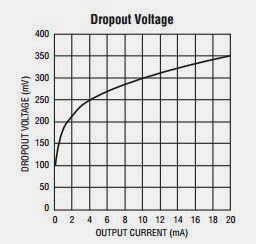
Dropout voltage - 350mV

For a linear regulator, as the output current from the regulator increases, drop out voltage increases which is shown in the graph below from datasheet of LT3014B


Let us assume i want a output voltage of 5V @20mA from LT3014B. To achieve this output, minimum input required is 5.35V. Let us assume, we are providing a input of 7.4V which is Li-ion standard battery pack voltage.

The power dissipated across the linear regulator is (7.4-5)*20m = 48mW

If the input is 50V and output is 5V, then power dissipated is (50-5)*20m = 0.9W

So, we can clearly see that as the difference between input and output is increasing in a linear regulator, power dissipation across regulator is going high. Also, imagine a case where input to output voltage difference is low but current is in amperes, in this case also, power dissipation across linear regulator is very high.

Important note: If the input to output voltage difference is high, or if the current output from regulator is high, power dissipation across linear regulator is very high in which case heat dissipation is high. We may need a huge heat sinks if we use linear regulators in such cases. Also, power is unnecessarily wasted.so, we have to go to switching regulator in these cases.

Power Dissipation calculation for LTM8020


I/P voltage range: 4-36V
O/P voltage range - 1.25-5V

The main factor to consider in switching regulators is efficiency. For a given load current, the efficiency can be calculated from the graph below as from LTM8020 datasheet.


To calculate power dissipation across switching regulator LTM8020, we have to take above graph into consideration. Let us assume my load is drawing 100mA for a input of 24V at output of 5V. In this case, from the graph efficiency is ~82%.

For above requirements, output power = 5v *100mA = 0.5W
Input required power = output/effeceincy = 0.5/0.82 = ~0.6W

So, power dissipated across LTM8020 is, 0.6-0,.5 = 0.1W

Important note: If either the input to output voltage difference is high, or if the current output from regulator is high, power dissipation across switching regulator is less in which case heat dissipation is less. We may not need a huge heat sinks if we use switching regulators in such cases. Also, power is not unnecessarily wasted.So, we have to go to switching regulator in these cases.