Saturday, 23 August 2014

Wireless Charging - The emerging trend

Many of us use a wall mount charger for charging out multimedia devices like smartphones, tablets, music devices, etc. These devices have a socket into which the external charger goes in. It is always recommended that you use a suggested charger for a specific device. What if you don't have to use this wired charger and charge your mobile hassle free? Yes, this is what wireless charging is. Just place your mobile on a charging pad and your mobile gets charged, as simple as that.

Wireless charging is based on the principle of magnetic induction. Magnetic induction meant there will be two coils in which the first coil (transmitter) has a current flowing through it which causes magnetic flux. when the second coil (receiver) is placed near to first coil the magnetic flux induces current in the second coil. So, a charging pad on which you place the mobile will have a coil in which flux will be developed. When you place your mobile right next to the charging pad, which has a second coil , it induces current and hence battery charges. Basically, it is the electromagnetic field that plays a role here.

An alternative to magnetic induction is resonant charging. In this the receiver need not be next to the transmitter. Both of them work on the principle of resonance. In this way of charging power is transmitted wireless at a 6.78 MHz rate. In this case, the resonance helps charging.

What are the various wireless charging standards?
  • A4WP (Alliance for wireless power)
  • PMA (Power Matter Allaince)
  • WPC (Wireless power consortium)

WPC developed Qi standard which is the most popular now and is in use. Qi is basically the magnetic induction type of charging. Regulatory approvals are in place for this standard.
A4WP developed resonant type charging. Regulatory approvals not in place.

What are the challenges from the designer point of view?

Let us take a smartphone designer, who wants to implement wireless charging in his device. The challenge for him is to select a chipset which is used as receiver. The chip has to support the desired standard. Also, the charging control circuitry to be implemented to connect to unit to be charged (battery). Chip sets are also available in the market which supports various charging standards. Coupling factor is of primary importance. A higher coupling factor leads to faster charging rate.

What are the various vendors for wireless charging chips?
  • IDT
  • Broadcom
  • NXP
  • Texas Instruments
  • Freescale
  • STMicroelectronics
What are the various domains wireless charging is expected to get exposed to?
  • Smartphone charging where the charge pads can be mounted outdoors at public places like bus stops, cafeterias.
  • Electric vehicles charging (Battery)
What are the differences between Inductive charging and resonant charging?
  • For inductive charging, the receiver must be in the close proximity of transmitter (receiver and transmitter separated by centimeter distance) where as for resonant charging this is not the case.
  • Coupling factor is high in inductive charging
  • Size of the coils is more in inductive charging than resonant charging
  • Cost is also high for inductive charging than resonant charging
  • Efficiency is high in inductive charging
  • Heat is more in inductive charging

Sunday, 27 July 2014

Soldering Techniques

We might have heard about soldering techniques used by manufacturers to place/solder components on a bare PCB. For an experienced guy, these techniques are familiar but for a fresher these all look like hard stuff which add to the additional burden of learning. The two most terminologies you hear from manufacturing industry are wave soldering and re-flow soldering. If PCB is not so complex and if you are getting your PCB s soldered at your local manufacturing locations you may not be hearing more about re-flow soldering. Let us look at the major differences between these two techniques.

Wave soldering:

Wave soldering is used to solder both through hole and SMD also. But this technique may not be suitable for most of the SMD components. Even in this era of surface mount technology, there are many applications which demand through hole components. So, wave soldering is a popularly used technique.

Reflow soldering:

Reflow soldering is mainly used for surface mount components. Even the through hole component soldering can be done with this technology. In this soldering technique, a solder paste is added to the PCB to glue the components upon which is the PCB is exposed to a controlled temperature environment. Check the datasheets before selecting the component and check your manufacturing facilities in parallel to give a manufacturing guideline for maximum reflow temperature to be used. Reflow machines can be of infrared type or conventional type.

What are the latest technologies?

Now-a-days embedded market is growing faster enabling the technology to be used at every step. SMT reflow machines are having lots of inventions incorporated and are coming up with latest technologies. some of the important observations are:

  • Graphical view of the temperature using a display attached 
  • Touch based screens for control activities
  • Minute temperature adjustment 
  • Complete process level data logging
  • Advanced cooling strategies
  • Efficient flux distribution techniques
  • Tracking the PCB from insertion to completion
  • Power consumption reduction in latest machines
  • Alarms for security
  • Remote control
What are the advantages of latest innovations?
  • Less maintenance costs
  • Exceptional thermal performance
  • Labour reduction
  • Automation
  • Quick turnout and hence high throughput
  • Controlled environment
  • Less chance of failures
  • Report generation at every step

Thursday, 10 July 2014

Understanding Oscilloscope Specifications - Part 2

Oscilloscopes can be said like heart of electronics testing especially protocol and high speed signals testing. Now a days oscilloscopes come with integrated test benches which help analyze high speed signals like USB, SATA, etc. These inbuilt test benches analyze signal specifications to the minute level and give a complete test report as a package. As a tester, this adds lot of flexibility and helps built confidence on the design. For a tester using oscilloscope initial challenge lies in understanding  specifications of it and selecting a right one for his application. 

Types of oscilloscopes:

The modern oscilloscopes come in various form factors which can be as big as bench-top to as well as wearable type and  middle level as hand-held type/pocket type. Hand held, pocket and wearable types are a very good addition to the field application engineers. That heavy packing, fright charges for a field engineer are no more a burden. The only disadvantage with these portable scopes is that their bandwidth is very less. So, the extent of debugging that can be done by the field engineer with these scopes is very limited. Even with such limitation, it is worth having one with you. Some people always have an eye on the pricing and cost wise they are nothing to worry as most of them are available in the range of $100 to $300. There are oscilloscopes especially designed for debugging phones during development.

Range of bandwidths:

Based on the domain you work on the oscilloscope varies. If you are working on a very low end digital signals and buses like SPI, I2C, SMBUS and UART, you don't need a very high end oscilloscope. The bandwidth requirement for such applications is very less and a 100 MHz bandwidth scope like TDS2014C works very much in such cases. If you are working on high end RF to high end digital signal signals, high bandwidth scopes are a necessity and be careful in choosing bandwidth of scope based on highest frequency to be measured. If you want to measure a frequency of 2.5 GHz, you must have a scope of bandwidth of at least 7.5 GHz. Today oscilloscopes are available up to 100 GHz. 

Waveform Generation:

One of the feature of oscilloscope is you have a output port which outputs fixed frequency signal. Hence, an oscilloscope can also be used in case you need a reference frequency for testing.  

Sunday, 15 June 2014

Power dissipation calculation for Linear and Switching regulators

For any hardware designer, power consumption control is a big challenge. Lower the power consumption of your product higher the success rate. For a battery operated devices like mobile, tablet and other smart devices power consumption is a critical specification. One critical component in this power consumption/wastage across the board is regulator. Power from the main source like battery, usb power is distributed across the board using regulators. Regulators can either step-up or step-down the input a DC voltage. Based on our requirement we choose a regulator type.

Regulators used in embedded hardware boards can be mainly classified as linear and switching regulators. There are several sub classifications in linear and switching regulators which we will discuss later. For now let us calculate the power dissipation calculation across Linear and switching regulator. For this we will take an example of devices from Linear technologies.

Linear Regulator: LT3014B
Switching Regulator: LTM8020

Power Dissipation calculation for LT3014B

I/P voltage range: 3V-80V
O/P voltage range - 1.22V-60V
Dropout voltage - 350mV

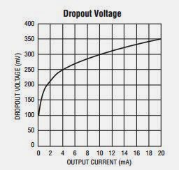
For a linear regulator, as the output current from the regulator increases, drop out voltage increases which is shown in the graph below from datasheet of LT3014B


Let us assume i want a output voltage of 5V @20mA from LT3014B. To achieve this output, minimum input required is 5.35V. Let us assume, we are providing a input of 7.4V which is Li-ion standard battery pack voltage.

The power dissipated across the linear regulator is (7.4-5)*20m = 48mW

If the input is 50V and output is 5V, then power dissipated is (50-5)*20m = 0.9W

So, we can clearly see that as the difference between input and output is increasing in a linear regulator, power dissipation across regulator is going high. Also, imagine a case where input to output voltage difference is low but current is in amperes, in this case also, power dissipation across linear regulator is very high.

Important note: If the input to output voltage difference is high, or if the current output from regulator is high, power dissipation across linear regulator is very high in which case heat dissipation is high. We may need a huge heat sinks if we use linear regulators in such cases. Also, power is unnecessarily wasted.so, we have to go to switching regulator in these cases.

Power Dissipation calculation for LTM8020


I/P voltage range: 4-36V
O/P voltage range - 1.25-5V

The main factor to consider in switching regulators is efficiency. For a given load current, the efficiency can be calculated from the graph below as from LTM8020 datasheet.


To calculate power dissipation across switching regulator LTM8020, we have to take above graph into consideration. Let us assume my load is drawing 100mA for a input of 24V at output of 5V. In this case, from the graph efficiency is ~82%.

For above requirements, output power = 5v *100mA = 0.5W
Input required power = output/effeceincy = 0.5/0.82 = ~0.6W

So, power dissipated across LTM8020 is, 0.6-0,.5 = 0.1W

Important note: If either the input to output voltage difference is high, or if the current output from regulator is high, power dissipation across switching regulator is less in which case heat dissipation is less. We may not need a huge heat sinks if we use switching regulators in such cases. Also, power is not unnecessarily wasted.So, we have to go to switching regulator in these cases.

Saturday, 14 June 2014

Diodes - Part 1 (Button diode, Cell diode, Pressfit diode)

Engineers outside automotive domain might never have thought how a automotive battery gets charged. A hardware engineer in automotive is very much familiar of those technical details. The whole mechanism happens with the help of alternators which convert mechanical energy to electrical energy. The electrical energy generated at this point is alternating one. So, either to charge the battery or to provide the power to the ECU (Engine control unit). So, rectification has to happen. The process of rectification converts alternating current to direct current. For these purpose we use rectifier diodes.


Button diode, Cell diode and Press fit diode are types of rectifier diodes used in rectification process. These are especially designed for automotive applications.

Advantages of rectifier diodes (Button type, Press fit, Cell diode) used in automotive applications:
  • Low leakage
  • High reverse voltage rating
  • Low cost
  • High surge current handling capability
  • High operating temperature
  • Plastic Casing on these diodes meet flammability standards

Thermal paste/compound - A small note

Thermal paste is a heat sink compound used on top of the processors (whether it be graphical or central processor), regulators for heat to follow smoothly to external medium. The mechanical designers suggest using a heat sink based on the thermal calculations. The principal behind using a heat sink in that the operating temperature of the device should not exceed the maximum specified ratings in the datasheet.

Operating temperature of a specific heat generating device is calculated by summation of junction temeparature and heat generated (Heat generated is the product of thermal resistance and power of operation). When this sum exceeds operating temperature specification that effect is catstrophic and can lead to device failure.

So, we have to use heat sink on top to enable the heat to escape from the device. Keep in mind that thermal paste is filling the imprefections of heat sink. The heat sink will be mounted on top of the device. Even though the heat sink is placed on top of device touching it there will be a air gap in between. Air is always a poor conductor of heat in which case another media must enable smooth heat flow. For this purpose we use a thermal paste. Thermal paste is a highly heat conductive paste.You mave have a large heat sink with exception fin structure for smooth heat flow, but, without a thermal paste the entire cost you have put on heat sink is a mere waste.

The thermal paste applied on top can be of different types. These can be electrically conductive as well as non-conductive. In a electronic board, it is always prefferable to use a non-conductive type. Cermaic based paste is one type of thermal paste. Arctic silver is the most preffered thermal paste.

What is Integrated Heat Spreader?
Keep in mind that the modern processors have a metal kind of enclosure for heat flow assistance. This we call a integrated heat spreader (IHS).

I already have a heat sink compound on the device. How do i clean it?
Usin Isopropyl Alcohol. Use a isopropyl dipped smooth cloth to rub off the paste.

Conformal coating for PCB

Engineers who worked on hadware boards which have to operate very low temperatures might not have come across conformal coating requirement. But who work on marine, defence, military, aerospace domains and hardware board designers who worked on board designs which have to work up to high temperatures and humidity might have used conformal coating. Now a days we can see conformal coating being used very extensively across other domains also (Telecomm, industrial, automotive, instrumentation). We can say that where there is a need for reliability and high protection conformal coating of PCB is a must.

Conformal coating is a chemical coating on top of the assmebled PCB which helps electronics to get shielded against harsh environments. If you have seen some relays, transformers available in the market, they have a plastic enclosure for internal electronics with a gel compound filled for protection against shock, vibration, stress, thermal, corrosion, moisture. This is what we call "plotting". You can see the huge black ics in the below figure.


Plotting is an expensive technique and conformal coating helps to achieve the protection simpler. The also disadvantage is that specific temperatures are used to form the protective layer which may cause the electronics to loose bonding. Conformal coating also adds dielectric strength to the PCB. Also, conformal coating ensures board reliability. Conformal coating can protect electroincs boards against the following problems:
  • Temperature (which we call thermal cycling in environmental tests)
  • Humidity
  • Moisture
  • Mechanical stress
  • Dust accumulation
  • Fungus formation
  • Corrosion because of salt spray
  • Shock & Vibration
  • Chemical contamination
There are specifications available forconformal coating guidelines especially in military and aerospace. For example, MIL-1-46058 is one such sytndard. Silicone is the most commonly used conformal coating material used for protection against high temperatures.

What are the various other conformal coating materials available?
Silicone, Epoxy, Acrylic, Urethane, Parylene. Urethane is the most widely used.

Once conformal coated, can we remove it?
Yes, it can be removed and there are several techniques available. Approach the manufacturer to get to know the type of material used and technique to remove coating. Acrylics are the easiest to remove.

What care need to be taken for resoldering a component on already conformally ciated PCB?
Once conformally coated, very high temperature must be applied by soldering machine to remove that coating. This may cause SMT pads to get lifted. In susch cases, careful attention must be provided while aplying temperature beyond certain range. Also, once rework is done take care that conformal coating residue is not present on the board which can give a problem in the long term. Take care of ESD which performing such procedures for removing conformal coating.

What can be the thickness of conformal coating?
Have seen a conformal coating of thickness up to 50um.

What are the advantages of conformal coating?
  • Eliminates need for costly mechanical enclosures
  • Less weight
  • Easy removal
What are the techniques used for conformal coating?
  • Brush
  • Spray
  • Dip
  • Automated
What care need to be taken for conformal coating?
Eliminate any surace defects. This means you have to equally spray without any gaps
Chose the conforming material as per the application and requirement
Choose the conformal coating technique as per expertise available
The drying process after coating must be simple. Can be air dired, normal dried or UV dried.
Coating material complies to industrial standards and is environmental friendly

How can suraface defects be detected in conformal coating?
Using UV light inspection